| CPC G09G 3/3266 (2013.01) [G09G 3/3233 (2013.01); G09G 2300/043 (2013.01); G09G 2300/0426 (2013.01); G09G 2300/0819 (2013.01); G09G 2300/0852 (2013.01); G09G 2310/0202 (2013.01); G09G 2310/0286 (2013.01); G09G 2310/08 (2013.01); G09G 2320/0233 (2013.01); G09G 2330/021 (2013.01)] | 18 Claims |
|
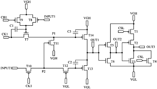
1. A shift register unit, comprising:
an input circuit, a first control circuit, a second control circuit, and an output circuit, wherein
the input circuit is connected with a first clock signal line, a second clock signal line, a first input terminal, a first power line, a first control node, and a second control node, and is configured to provide a signal of the first input terminal to the second control node under control of the first clock signal line and provide a signal of the first clock signal line or the first power line to the first control node under control of the second clock signal line, the first input terminal, and the second control node;
the first control circuit is connected with the first control node, the second control node, the first power line, a second power line, and a first output terminal, and is configured to provide a signal of the first power line or the second power line to the first output terminal under control of the first control node and the second control node;
the second control circuit is connected with the first power line, the second power line, the first output terminal, and a second output terminal, and is configured to provide an effective level signal of the first power line or the second power line to the second output terminal under control of the first output terminal; and
the output circuit is connected with a control signal line, the first power line, the second power line, the second output terminal, and a third output terminal, and is configured to output an effective level signal of the first power line or the second power line to the third output terminal under control of the control signal line and the second output terminal, wherein, within the time of one frame, a duration of an effective level signal provided by the third output terminal is longer than a duration of an effective level signal provided by the second output terminal;
wherein the output circuit comprises a first output sub-circuit and a second output sub-circuit;
the first output sub-circuit is connected with the control signal line, the first power line, the second output terminal, and the third output terminal, and is configured to provide the effective level signal of the first power line to the third output terminal under the control of the control signal line and the second output terminal; and
the second output sub-circuit is connected with the control signal line, the second power line, the second output terminal, and the third output terminal, and is configured to provide the effective level signal of the second power line to the third output terminal under the control of the control signal line and the second output terminal;
wherein the first output sub-circuit comprises a first transistor and a second transistor; a control electrode of the first transistor is connected with the control signal line, a first electrode of the first transistor is connected with the first power line, and a second electrode of the first transistor is connected with a first electrode of the second transistor; a control electrode of the second transistor is connected with the second output terminal, and a second electrode of the second transistor is connected with the third output terminal;
the second output sub-circuit comprises a third transistor and a fourth transistor; a control electrode of the third transistor is connected with the second output terminal, a first electrode of the third transistor is connected with the second power line, and a second electrode of the third transistor is connected with the third output terminal; and a control electrode of the fourth transistor is connected with the control signal line, a first electrode of the fourth transistor is connected with the second power line, and a second electrode of the fourth transistor is connected with the third output terminal.
|