| CPC G09G 3/3266 (2013.01) [G09G 2300/0408 (2013.01); G09G 2310/08 (2013.01); G09G 2330/021 (2013.01)] | 19 Claims |
|
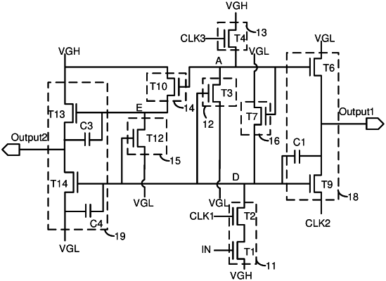
1. A gate on array unit circuit comprising:
an input sub-circuit connected to a first node and configured to set a turn-on voltage level to the first node in response to an input signal and a first clock signal;
a first pull-down sub-circuit connected to a second node and the first node, and configured to pull down a voltage level at the second node to a turn-off voltage level in response to the turn-on voltage level at the first node;
a pull-up sub-circuit connected to the second node and configured to set the turn-on voltage level to the second node in response to a third clock signal;
a first control sub-circuit connected to the second node and a third node and configured to set a turn-on voltage level to the third node in response to the turn-on voltage level at the second node;
a second control sub-circuit connected to the first node and the third node, and configured to set a turn-off voltage level to the third node in response to the turn-on voltage level at the first node;
a first output sub-circuit configured to output a first output signal at the turn-on voltage level triggered by a second clock signal through one period of a cycle time associated with the input signal in response to voltage levels at the second node and the first node; and
a second output sub-circuit configured to output a second output signal falling to the turn-off voltage level triggered by the first clock signal through at least the same one period of the cycle time before rising to the turn-on voltage level triggered by the third clock signal in response to voltage levels at the first node and the third node;
wherein the second output sub-circuit comprises a thirteenth transistor, a fourteenth transistor, a third capacitor, and a fourth capacitor, the thirteenth transistor, the fourteenth transistor and the third capacitor are respectively coupled to a second output terminal for outputting the second output signal; the thirteenth transistor having a first terminal configured to receive a first voltage signal set at the turn-on voltage level, a gate terminal coupled to the third node, and a second terminal coupled to the second output terminal; the fourteenth transistor having a first terminal configured to receive a second voltage signal set at the turn-off voltage level, a gate terminal coupled to the first node, and a second terminal coupled to the second output terminal; the third capacitor having a first terminal coupled to the third node and a second terminal coupled to the second output terminal; and the fourth capacitor having a first terminal coupled to the first node and a second terminal coupled to the first terminal of the fourteenth transistor.
|