| CPC G09G 3/3233 (2013.01) [G09G 2300/0408 (2013.01); G09G 2300/0426 (2013.01); G09G 2300/0809 (2013.01); G09G 2310/08 (2013.01)] | 16 Claims |
|
1. A display substrate, comprising: a display region and a non-display region, wherein the display substrate comprises: a substrate, and a first power supply line, a scanning signal line, a first initial signal line and a plurality of display units disposed on a substrate; the display units are located in the display region, and the first power supply line is located in the non-display region;
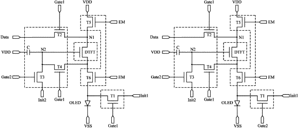
a display unit comprises: a drive structure layer and a light-emitting structure layer; the light-emitting structure layer comprises: a light-emitting element, and the drive structure layer comprises: a pixel drive circuit configured to drive the light-emitting element to emit light; the pixel drive circuit comprises: a reset sub-circuit, connected with the scanning signal line, the first initial signal line and a first electrode of the light-emitting element respectively, and configured to provide a signal of the first initial signal line to the first electrode of the light-emitting element under control of a signal of the scanning signal line to initialize the first electrode of the light-emitting element; and a second electrode of the light-emitting element is connected with the first power supply line; and
the first initial signal line is electrically connected with the first power supply line;
wherein the scanning signal line comprises: a first scanning signal line and a second scanning signal line disposed in parallel; the display substrate also comprises: a second power supply line, a light-emitting signal line, a data signal line and a second initial signal line;
the pixel drive circuit further comprises: a drive control sub-circuit, a drive sub-circuit and a light-emitting control sub-circuit;
the reset sub-circuit comprises: a first transistor; the drive control sub-circuit comprises: a storage capacitor, second to fourth transistors; the drive sub-circuit comprises: a drive transistor; and the light-emitting control sub-circuit comprises a fifth transistor and a sixth transistor;
the drive structure layer comprises: a first insulating layer, a semiconductor layer, a second insulating layer, a first metal layer, a third insulating layer, a second metal layer, a fourth insulating layer, and a third metal layer which are sequentially stacked on the substrate; and
the semiconductor layer comprises: an active layer of all transistors in the pixel drive circuit the first metal layer comprises: the first scanning signal line, the second scanning signal line, the light-emitting signal line and control electrodes of all transistors in the pixel drive circuit the second metal layer comprises: the first initial signal line and the second initial signal line; the third metal layer comprises: the first power supply line, the second power supply line, the data signal line and the first and second electrodes of all transistors in the pixel drive circuit.
|