| CPC G09G 3/3233 (2013.01) [G09G 2300/0426 (2013.01); G09G 2300/0819 (2013.01); G09G 2300/0842 (2013.01); G09G 2310/08 (2013.01); G09G 2320/029 (2013.01); G09G 2320/045 (2013.01); G09G 2330/08 (2013.01); G09G 2330/10 (2013.01); G09G 2330/12 (2013.01)] | 15 Claims |
|
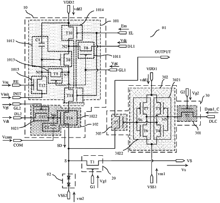
1. A pixel driving circuit, comprising:
a driving sub-circuit configured to supply a driving signal to an element to be driven;
a detection sub-circuit electrically connected to a detection control signal terminal and a detection node, and configured to detect a voltage value of the detection node in response to a detection control signal received at the detection control signal terminal, wherein the detection node is equivalent to a point on a connection line between the driving sub-circuit and the element to be driven; and
a compensation sub-circuit electrically connected to a compensation control signal terminal, a compensation data signal terminal, the detection node and a compensation output terminal; the compensation sub-circuit is configured to transmit the driving signal supplied by the driving sub-circuit from the detection node to the compensation output terminal according to a first compensation data signal received at the compensation data signal terminal and in response to a compensation control signal received at the compensation control signal terminal; wherein
the compensation sub-circuit includes: an input unit, a storage unit and a compensation control unit, wherein
the input unit is electrically connected to the compensation control signal terminal, the compensation data signal terminal and the storage unit, and is configured to write the first compensation data signal into the storage unit in response to the compensation control signal;
the storage unit is further electrically connected to the compensation control unit, and is configured to generate and store a second compensation data signal according to the written first compensation data signal, and to output the second compensation data signal to the compensation control unit; and
the compensation control unit is further electrically connected to the detection node and the compensation output terminal, and is configured to turn on a connection circuit between the detection node and the compensation output terminal in response to the second compensation data signal;
the compensation control unit includes a seventh transistor, wherein a control electrode of the seventh transistor is electrically connected to the storage unit, a first electrode of the seventh transistor is electrically connected to the detection node, and a second electrode of the seventh transistor is electrically connected to the compensation output terminal.
|