| CPC G09G 3/3225 (2013.01) [H10K 59/131 (2023.02); G09G 2300/0426 (2013.01); G09G 2300/0842 (2013.01); G09G 2310/061 (2013.01); G09G 2320/0233 (2013.01)] | 17 Claims |
|
1. An array substrate, comprising:
a substrate;
a pixel array disposed on the substrate, comprising a plurality of sub-pixels arranged in a plurality of rows and a plurality of columns, wherein each of the sub-pixels has a pixel circuit, and a data signal input terminal, a scan signal input terminal, and a driving reset control signal input terminal coupled to the pixel circuit, the pixel circuit comprises a data writing circuit, a driving circuit and a driving reset circuit, the driving circuit comprises a control terminal, a first terminal, and a second terminal, the data writing circuit is coupled to the data signal input terminal, the scan signal input terminal and the first terminal of the driving circuit, and is configured to provide a data signal to the first terminal of the driving circuit under a control of a scan signal, the driving circuit is configured to provide a driving current to a light-emitting device, and the driving reset circuit is coupled to the driving reset control signal input terminal, the control terminal of the driving circuit, and a reset voltage terminal, and is configured to reset the control terminal of the driving circuit under a control of the driving reset control signal;
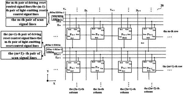
a plurality of pairs of scan signal lines, extending in a row direction and being spaced apart from each other in a column direction, wherein each of the plurality of pairs of scan signal lines comprises a first scan signal line and a second scan signal line, and a m-th pair of scan signal lines corresponds to the sub-pixels in a m-th row, where m is an integer greater than or equal to 1, and wherein the first scan signal line of the m-th pair of scan signal lines is configured to provide a first scan signal to the scan signal input terminal of the sub-pixel in a (2n−1)-th column from the sub-pixels in the m-th row, where n is an integer greater than or equal to 1, and the second scan signal line of the m-th pair of scan signal lines is configured to provide a second scan signal to sub-pixel in a 2n-th column from the sub-pixels in the m-th row; and
a plurality of pairs of driving reset control signal lines, extending in the row direction and being spaced apart from each other in the column direction, wherein each of the plurality of pairs of driving reset control signal lines comprises a first driving reset control signal line and a second driving reset control signal line, and a m-th pair of driving reset control signal lines corresponds to the sub-pixels in the m-th row,
wherein the first driving reset control signal line of the m-th pair of driving reset control signal lines is configured to provide a first driving reset control signal to the driving reset control signal input terminal of the sub-pixel in the (2n−1)-th column from the sub-pixels in the m-th row, and the second driving reset control signal line of the m-th pair of driving reset control signal lines is configured to provide a second driving reset control signal to the driving reset control signal input terminal of the sub-pixel in a 2n-th column from the sub-pixels in the m-th row of sub-pixels, and
the first scan signal line of the m-th pair of scan signal lines and the second driving reset control signal line of the m-th pair of driving reset control signal lines are one and the same signal line such that the first scan signal provided by the first scan signal line of the m-th pair of scan signal lines to the sub-pixel in the (2n−1)-th column from the sub-pixels in the m-th row is also used as the second driving reset control signal to the sub-pixel in the 2n-th column from the sub-pixels in the m-th row;
a plurality of light-emitting control signal lines, which extend in the row direction, and are spaced apart from each other in the column direction,
wherein the sub-pixel further comprises a light-emitting control signal terminal, and the pixel circuit further comprises a light-emitting control circuit,
wherein the light-emitting control circuit is coupled to the light-emitting control signal terminal, the first voltage terminal, the driving circuit, and the light-emitting device, and configured to apply a first voltage from the first voltage source to the driving circuit, and to apply a driving current generated by the driving circuit to the light-emitting device, and
wherein a m-th light-emitting control signal line is configured to be coupled to the light-emitting control signal terminals of the sub-pixels in the m-th row to provide the light-emitting control signal; and
a plurality of pairs of light-emitting reset control signal lines, which extend in the row direction and are spaced apart from each other in the column direction,
wherein the sub-pixel further comprises a light-emitting reset control signal input terminal, and the pixel circuit further comprises a light-emitting reset circuit, which is coupled to the light-emitting reset control signal input terminal, the reset voltage terminal, and the light-emitting device, and configured to reset the light-emitting device under a control of a light-emitting reset control signal,
wherein each of the plurality of pairs of light-emitting reset control signal lines comprises a first light-emitting reset control signal line and a second light-emitting reset control signal line, and a m-th pair of light-emitting reset control signal lines corresponds to sub-pixels in the m-th row, and
wherein the first light-emitting reset control signal line of the m-th pair of light-emitting reset control signal lines is configured to provide a first light-emitting reset control signal to the light-emitting reset control signal input terminal of the sub-pixel in the (2n−1)-th column from the sub-pixels in the m-th row, and the second light-emitting reset control signal line of the m-th pair of light-emitting reset control signal lines is configured to provide a second light-emitting reset control signal to the light-emitting reset control signal input terminal of the sub-pixel in the 2n-th column from the sub-pixels in the m-th row,
wherein the first light-emitting reset control signal line of the m-th pair of light-emitting reset control signal lines and the first driving reset control signal line of a (m+1)-th pair of driving reset control signal lines are one and the same signal line such that the first light-emitting reset control signal provided by the first light-emitting reset control signal line of the m-th pair of light-emitting reset control signal lines to the sub-pixel in the (2n−1)-th column from the sub-pixels in the m-th row is also used as the first driving reset control signal of the sub-pixel in the (2n−1)-th column from the sub-pixels in the (m+1)-th row, and the second light-emitting reset control signal line of the m-th pair of light-emitting reset control signal lines and the second driving reset control signal line of the (m+1)-th pair of driving reset control signal lines are one and the same signal line such that the second light-emitting reset control signal provided by the second light-emitting reset control signal line of the m-th pair of light-emitting reset control signal lines to the sub-pixel in the 2n-th column from the sub-pixels in the m-th row is also used as the second driving reset control signal of the sub-pixel in the 2n-th column from the sub-pixels in the (m+1)-th row.
|