| CPC G09G 3/20 (2013.01) [G11C 19/28 (2013.01); G09G 2300/0408 (2013.01); G09G 2310/0267 (2013.01); G09G 2310/0286 (2013.01); G09G 2310/061 (2013.01); G09G 2330/021 (2013.01)] | 8 Claims |
|
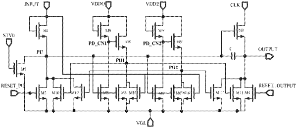
1. A gate driving circuit, comprising M shift registers and N clock signal lines; every N adjacent shift registers among the M shift registers being respectively connected to the N clock signal lines, where N is an even number greater than, and M is an integer greater than or equal to N;
wherein each of the M shift registers at least comprises an input sub-circuit, an output sub-circuit and a pull-up reset sub-circuit; in response to an input signal input by a signal input terminal, the input sub-circuit writes the input signal into a pull-up node; in response to a potential of the pull-up node, the output sub-circuit outputs a clock signal input by a clock signal terminal through a signal output terminal; and in response to a pull-up reset signal input by a pull-up reset signal terminal, the pull-up reset sub-circuit resets the potential of the pull-up node through a turn-off level signal;
a signal output terminal of an ith shift register is connected to a signal input terminal of a (i+p)th shift register, where (N−4)/2≤p≤N/2, and i is taken from 1 to (M−p);
a pull-up reset signal terminal of a jth shift register is connected to a signal output terminal of a (j+q)th shift register, where 1<q−p<N/2, and j is taken from 1 to (M−q);
wherein each of the shift registers further comprises an output reset sub-circuit and in response to an output reset signal input by an output reset signal terminal, the output reset sub-circuit resets the signal output terminal through the turn-off level signal;
wherein an output reset signal terminal of a kth shift register is connected to a signal output terminal of a (k+p)th shift register, where k is taken from 1 to (M−p);
wherein the output reset signal terminal is configured to reset only the signal output terminal; and
wherein the output sub-circuit is configured to operate for a delay of ⅖ of one period of the clock signal.
|