| CPC G09G 3/20 (2013.01) [G11C 19/28 (2013.01); G09G 2310/0286 (2013.01)] | 20 Claims |
|
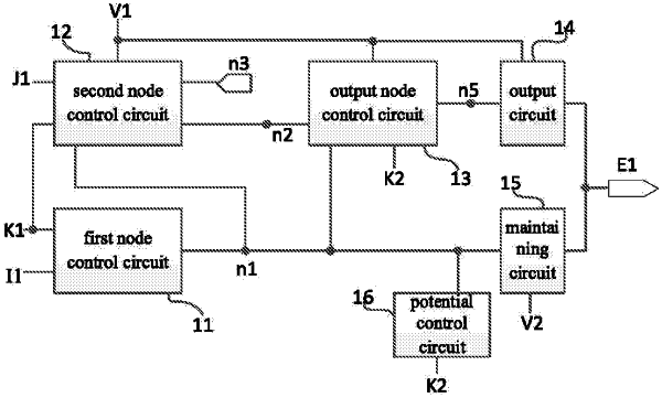
1. A shift register unit comprising a first node control circuit, a second node control circuit, an output node control circuit, an output circuit, a maintaining circuit, and a potential control circuit, wherein:
the first node control circuit is electrically connected to a first clock signal terminal, an input terminal, and a first node, and is configured to control the connection between the input terminal and the first node under the control of a first clock signal provided by the first clock signal terminal;
the second node control circuit is electrically connected to a node control terminal, the first clock signal terminal, a first voltage terminal, the first node, a second node, and a third node, respectively, is configured to control a potential of the third node according to a potential of the node control terminal, a first voltage signal provided by the first voltage terminal, and the first clock signal, and control a potential of the second node according to the first clock signal and the first voltage signal under the control of the potential of the third node and a potential of the first node;
the output node control circuit is electrically connected to the first node, the second node, a second clock signal terminal, an output node, and the first voltage terminal, respectively, and is configured to control a potential of the output node under the control of the potential of the second node and a second clock signal provided by the second clock signal terminal according to the second clock signal, and control the connection between the output node and the first voltage terminal under the control of the potential of the first node, and is configured to maintain the potential of the output node;
the output circuit is electrically connected to the output node, the first voltage terminal, and an output terminal, respectively, is configured to control the connection between the output terminal and the first voltage terminal under the control of the potential of the output node;
the potential control circuit is electrically connected to a control terminal of the maintaining circuit and the second clock signal terminal, respectively, is configured to control a potential of the control terminal of the maintaining circuit according to the second clock signal;
the control terminal of the maintaining circuit is electrically connected to the first node, the maintaining circuit is also electrically connected to the output terminal and the second voltage terminal, is configured to control the connection between the output terminal and the second voltage terminal under the control of a potential of the control terminal of the maintaining circuit.
|