| CPC G06N 3/063 (2013.01) [G06N 3/065 (2023.01); G11C 11/24 (2013.01); G11C 11/54 (2013.01); G11C 27/005 (2013.01)] | 8 Claims |
|
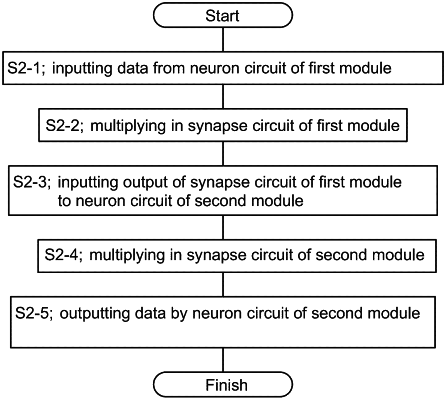
1. A semiconductor device comprising a first module and a second module,
wherein the first module comprises a first circuit and a second circuit,
wherein the first circuit comprises a selector circuit,
wherein the first circuit is selectively configured to output a first analog signal to the second circuit through the selector circuit, and to convert the first analog signal from current to voltage and output the first analog signal to the second module through the selector circuit,
wherein the second circuit comprises an analog memory, a first multiplier circuit, and a second multiplier circuit,
wherein the analog memory is configured to store a data,
wherein the first multiplier circuit is configured to generate a second signal that is obtained by weighting of the first analog signal according to the data, and
wherein the second multiplier circuit is configured to update the data in the analog memory.
|