| CPC G06K 19/0718 (2013.01) [G06K 19/077 (2013.01); G06K 19/0715 (2013.01); G06K 19/0723 (2013.01); H02M 3/33507 (2013.01); H02M 3/33584 (2013.01)] | 16 Claims |
|
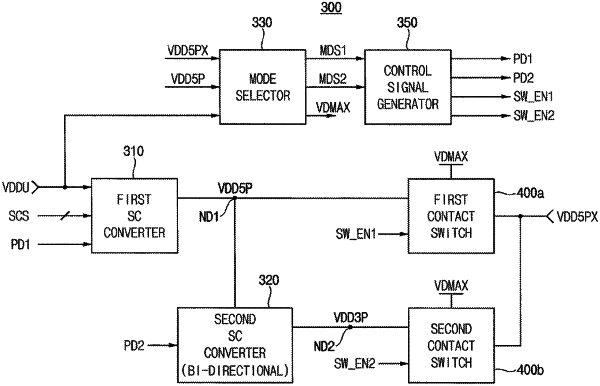
1. An internal voltage generation circuit of a smart card configured to perform a fingerprint authentication, the internal voltage generation circuit comprising:
a first contact switch configured to selectively switch a contact voltage received from an external card reader to a first node based on a first switching enable signal, in a contact mode;
a second contact switch configured to selectively switch the contact voltage to a second node based on a second switching enable signal, in the contact mode;
a switched capacitor converter configured to step down a contactless voltage induced by an electromagnetic wave received from the card reader to provide a contactless mode first driving voltage to the first node;
a bidirectional switched capacitor converter, connected to the first node and the second node, the bidirectional switched capacitor converter configured to:
in a contactless mode, step down the contactless mode first driving voltage at the first node to provide a contactless mode second driving voltage to the second node; and
in the contact mode, either step down a contact mode first driving voltage at the first node to provide a contact mode second driving voltage to the second node, or boost a contact mode second driving voltage at the second node based on a level of the contact voltage to provide a boosted voltage to the first node;
a mode selector configured to output a first mode signal and a second mode signal, the first mode signal designating one of the contact mode and the contactless mode, the second mode signal designating one of a plurality of sub-modes of the contact mode, the mode selector further configured to select a highest voltage among the contact voltage, the contactless voltage and the contactless mode first driving voltage or the contact mode first driving voltage to output the selected voltage as a control voltage; and
a control signal generator configured to generate a first power-down signal that enables/disables the switched capacitor converter, a second power-down signal that enables/disables the bidirectional switched capacitor converter, the first switching enable signal and the second switching enable signal, based on the first mode signal and the second mode signal.
|