| CPC G06F 3/0611 (2013.01) [G06F 3/0659 (2013.01); G06F 3/0673 (2013.01); G06F 12/0877 (2013.01); G06F 2212/60 (2013.01)] | 20 Claims |
|
11. A method comprising:
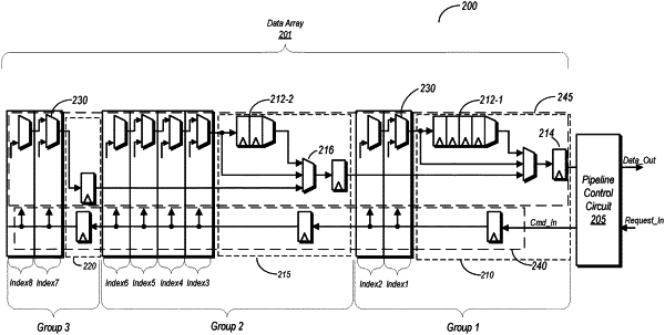
initiating, using a pipeline control circuit, cache memory accesses for data from a cache memory circuit, wherein the cache memory circuit includes a data array arranged into a plurality of groups having minimum access latencies with different numbers of clock cycles than other ones of the plurality of groups, wherein a minimum access latency for a particular one of the plurality of groups is dependent on its distance from the pipeline control circuit, and wherein an access latency for a given cache memory access is bounded to a maximum access latency by a plurality of latency control circuits;
receiving first data, from a first one of the plurality of groups, at a first one of the plurality of latency control circuits associated with a first one of the plurality of groups;
receiving second data at the first one of the plurality of latency control circuits from a second one of the plurality of groups that is more distant from the pipeline control circuit than the first one of the plurality of groups;
forwarding, in a first clock cycle and using the first one of the plurality of latency control circuits, the second data rather than first data from the first one of the plurality of groups when both the first and second data are concurrently available; and
storing the first data, in the first one of the plurality of latency control circuits, for forwarding during a clock cycle subsequent to the first clock cycle.
|