| CPC G06F 3/0611 (2013.01) [G06F 3/0635 (2013.01); G06F 3/0679 (2013.01)] | 26 Claims |
|
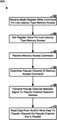
19. A pseudo channel based memory system, comprising a plurality of pseudo channels, including a first pseudo channel,
wherein the pseudo channel based memory system is configured to:
receive a memory access command targeting the first pseudo channel;
use a first pseudo channel data bus and a second pseudo channel data bus concurrently to implement the memory access command; and
receive a mode register write command configured to cause the pseudo channel based memory system to handle a successive memory access command as a low latency type memory access command, wherein the memory access command targeting the first pseudo channel is a successive memory access command to the mode register write command.
|