| CPC G06F 3/04164 (2019.05) [G06F 3/0412 (2013.01); G06F 3/0446 (2019.05); G06F 2203/04107 (2013.01)] | 20 Claims |
|
1. A touch display device, comprising:
a touch display module including a display screen and a touch panel; wherein a display driving circuit is disposed on the display screen, and a plurality of electrode leads are disposed in a peripheral area of the touch panel;
a flexible printed circuit electrically connected to the touch display module; and
a touch chip disposed on the flexible printed circuit;
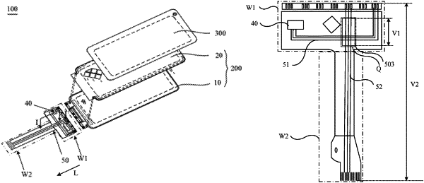
wherein the flexible printed circuit has a body area and a connection area located on a side of the body area; the flexible printed circuit includes:
a first flexible substrate including a first surface and a second surface arranged opposite to each other;
a first metal pattern layer located on a side of the first flexible substrate where the first surface is located; wherein the first metal pattern layer includes a plurality of first touch wirings electrically connected to the touch chip;
a second metal pattern layer located on the second surface of the first flexible substrate; wherein the second metal pattern layer includes a plurality of data wirings electrically connected to the display driving circuit; and
a metal shielding layer located on the first surface of the first flexible substrate and located between the first flexible substrate and the first metal pattern layer; wherein the metal shielding layer is insulated from the first metal pattern layer; wherein a ratio of a longitudinal length, in a direction from the body area to the connection area, of the metal shielding layer to a longitudinal length, in the direction from the body area to the connection area, of the flexible printed circuit is in a range of 20% to 40%, inclusive;
wherein the first metal pattern layer and the second metal pattern layer have an overlapping area therebetween in a direction from the second surface to the first surface; the metal shielding layer is located at least in the overlapping area.
|