| CPC G06F 3/04164 (2019.05) [G06F 3/0412 (2013.01); G06F 3/0443 (2019.05); G06F 3/0446 (2019.05); G09F 9/30 (2013.01); G09G 2300/0413 (2013.01)] | 20 Claims |
|
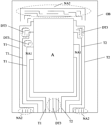
1. A display panel, comprising:
a base substrate, the base substrate comprising a display area and a non-display area around the display area;
a touch electrode layer on the base substrate, the touch electrode layer being within the display area; and
a plurality of signal lines electrically connected with the touch electrode layer, the plurality of signal lines being distributed within a first area of the non-display area adjacent to the display area,
wherein the display panel further comprises a plurality of outer dummy traces located within a second area of the non-display area, the second area being between the first area and an outer border of the non-display area,
wherein the plurality of outer dummy traces and the plurality of signal lines are separated from each other.
|