| CPC G03F 7/70775 (2013.01) [H01L 21/6838 (2013.01); H01L 21/68742 (2013.01)] | 12 Claims |
|
1. A device for adjusting a wafer, comprising:
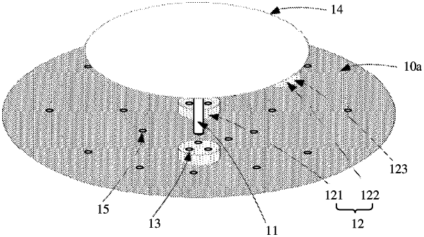
a lifting module, the lifting module comprising a first carrier surface configured to carry a wafer, and the first carrier surface ascending to a preset highest position or descending to a preset lowest position relative to a reference surface;
a carrier module, the carrier module comprising a plurality of carrier units, carrier surfaces of the plurality of carrier units constituting a second carrier surface, a position of the second carrier surface being higher than the preset lowest position and being lower than the preset highest position, and the second carrier surface being configured to receive and carry the wafer carried on the first carrier surface;
a base plate, a top surface of the base plate being used as the reference surface, the reference surface being lower than or being located at the preset lowest position; and
a suction module, the suction module comprising a plurality of first suction openings and a second suction opening, the plurality of first suction openings facing the wafer and each surrounded by the carrier surface of one of the plurality of carrier units, the second suction opening facing the wafer and surrounded by the reference surface, the suction module being configured to adsorb the wafer through the plurality of first suction openings and the second suction opening simultaneously, and the suction module being further configured to control a suction rate of the second suction opening, such that an adsorption force applied to the wafer through the second suction opening is less than an adsorption force applied to the wafer through the plurality of first suction openings;
wherein a plurality of centers corresponding to the plurality of first suction openings are located at a same circle, and a center of the second suction opening coincides with a circle center of the circle.
|