| CPC G02F 1/136222 (2021.01) [G02F 1/133512 (2013.01); G02F 1/136209 (2013.01); G02F 1/136227 (2013.01)] | 20 Claims |
|
1. A display panel, comprising an array substrate and a color filter substrate that are oppositely arranged; wherein
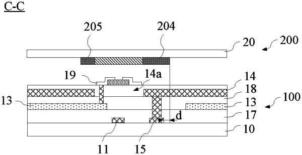
the array substrate comprises a first substrate, a common electrode, a plurality of auxiliary common electrodes, and a first insulating layer, wherein the first insulating layer is between the plurality of auxiliary common electrodes and the common electrode and is provided with via holes, and the auxiliary common electrodes are connected to the common electrode via the via holes; and
the color filter substrate comprises a second substrate and a black matrix pattern, wherein the black matrix pattern comprises a body, via hole shielding parts, and compensation shielding parts, both the via hole shielding part and the compensation shielding part being connected to the body, wherein
the body defines a plurality of sub-pixel regions arranged in an array on the second substrate, wherein each sub-pixel region comprises a first domain and a second domain, the first domains alternating with the second domains in a first direction in which the first domain and the second domain in a same sub-pixel region are arranged, and
the via hole shielding parts are disposed within the first domains of part of the plurality of sub-pixel regions, orthographic projections of the via holes on the first substrate are within orthographic projections of the via hole shielding parts on the first substrate, the compensation shielding parts are disposed within the second domains that are adjacent in the first direction to the first domains where the via hole shielding parts are disposed, and at most one of the via hole shielding part and the compensation shielding part is disposed in one sub-pixel region.
|