| CPC G02F 1/035 (2013.01) [G02B 6/13 (2013.01); G02B 2006/1204 (2013.01)] | 15 Claims |
|
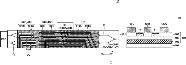
1. An optical device comprising:
a substrate;
a layered structure provided on the substrate, the layered structure including an intermediate layer, an optical waveguide formed of a thin crystal film having an electro-optic effect, and a buffer layer stacked in this order; and
an electrode provided on or above the buffer layer and configured to apply a direct current voltage to the optical waveguide,
wherein a resistivity of the intermediate layer is higher than a resistivity of the buffer layer, and the resistivity of the buffer layer is lower than a resistivity of the optical waveguide formed of the thin crystal film.
|