| CPC G02F 1/035 (2013.01) [G02F 1/225 (2013.01); G02B 2006/12142 (2013.01)] | 20 Claims |
|
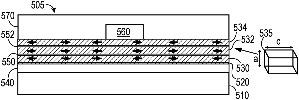
1. A wafer comprising:
a substrate comprising silicon or germanium;
a buffer layer coupled to the substrate and configured to relieve stress within the wafer; and
a layer stack disposed on a top surface of the buffer layer, the layer stack including:
a plurality of electro-optic material layers; and
a plurality of interlayers interleaved with the plurality of electro-optic material layers,
wherein the plurality of interlayers maintains a first lattice structure at a room temperature and at a cryogenic temperature; and
wherein the plurality of electro-optic material layers are under tensile stress and maintain a second lattice structure and crystallographic phase at the room temperature and the cryogenic temperature.
|