US 11,892,651 B2
Optically effective element, method of producing an optically effective element, and optoelectronic component
Roland Enzmann, Regensburg (DE); Hubert Halbritter, Dietfurt-Toeging (DE); Markus Arzberger, Sunnyvale, CA (US); Andreas Ploessl, Regensburg (DE); Roland Schulz, Regensburg (DE); Georg Rossbach, Regensburg (DE); Bernd Boehm, Obertraubling (DE); Frank Singer, Reganstauf (DE); and Matthias Sabathil, Regensburg (DE)
Assigned to OSRAM OLED GmbH, Regensburg (DE)
Filed by OSRAM OLED GmbH, Regensburg (DE)
Filed on Apr. 1, 2021, as Appl. No. 17/219,943.
Application 17/219,943 is a division of application No. 15/693,531, filed on Sep. 1, 2017, granted, now 10,996,482.
Claims priority of application No. 10 2016 116 747.9 (DE), filed on Sep. 7, 2016; application No. 10 2016 116 748.7 (DE), filed on Sep. 7, 2016; and application No. 10 2016 116 749.5 (DE), filed on Sep. 7, 2016.
Prior Publication US 2021/0223559 A1, Jul. 22, 2021
Int. Cl. G02B 27/09 (2006.01); G02B 5/18 (2006.01); G02B 3/00 (2006.01)
CPC G02B 27/0916 (2013.01) [G02B 3/0075 (2013.01); G02B 5/1814 (2013.01); G02B 5/1857 (2013.01); G02B 5/1866 (2013.01); G02B 27/0944 (2013.01); G02B 27/0961 (2013.01)] 30 Claims
OG exemplary drawing
 
1. An optoelectronic component comprising:
an optoelectronic semiconductor chip configured to emit electromagnetic radiation;
an optically effective element arranged such that electromagnetic radiation emitted by the optoelectronic semiconductor chip passes through the optically effective element; and
a housing,
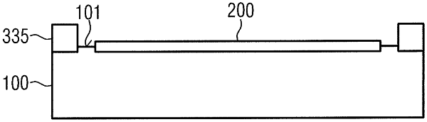
wherein the optoelectronic semiconductor chip is arranged in a cavity of the housing,
the optically effective element comprises a carrier,
a first optically effective structure arranged on a top side of the carrier, and
a cover arranged above the first optically effective structure,
wherein the optically effective element is arranged in the cavity of the housing.