| CPC G01S 7/4865 (2013.01) [G01S 7/4863 (2013.01); G01S 17/894 (2020.01); G06F 1/10 (2013.01); G06T 7/50 (2017.01); G06T 15/005 (2013.01); G06T 15/08 (2013.01); G06T 2207/10108 (2013.01)] | 22 Claims |
|
1. A depth map sensor comprising:
a first array of first pixels, each first pixel comprising a first photodetector associated with a first pixel circuit comprising a first plurality of bins for accumulating events;
a second array of second pixels, each second pixel comprising a second photodetector associated with a second pixel circuit comprising a second plurality of bins for accumulating events;
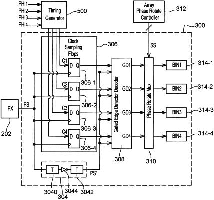
a clock source configured to generate a plurality of phase-shifted clock signals;
a first circuit having a plurality of first output lines coupled to the first array of first pixels, the first circuit configured to receive the plurality of phase-shifted clock signals, wherein the first circuit comprises a first sub-circuit and a second sub-circuit, the first sub-circuit configured to propagate the plurality of phase-shifted clock signals to the second sub-circuit during a first period determined by a first enable signal, wherein the propagation of the phase-shifted clock signals to the second sub-circuit is interrupted at an end of the first period and wherein the second sub-circuit is configured to select to which of the plurality of first output lines each of the plurality of phase-shifted clock signals is applied; and
a second circuit having a plurality of second output lines coupled to the second array of second pixels, the second circuit receiving the plurality of phase-shifted clock signals from the clock source, wherein the second circuit comprises a third sub-circuit and a fourth sub-circuit, the third sub-circuit configured to propagate the plurality of phase-shifted clock signals to the fourth sub-circuit during a second period determined by a second enable signal and the fourth sub-circuit configured to select to which of the plurality of second output lines each of the plurality of phase-shifted clock signals is applied, wherein a duration of the second period is different from a duration of the first period.
|