| CPC G01R 31/31705 (2013.01) [G01R 31/31726 (2013.01); G01R 31/318597 (2013.01)] | 22 Claims |
|
1. A processing system comprising:
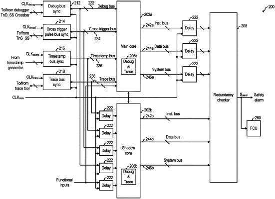
a main processing core comprising a main functional core and a main debug circuit, the main debug circuit having a debug input coupled to a debug bus and a debug output coupled to the debug bus;
a shadow processing core comprising a shadow functional core and a shadow debug circuit, the shadow debug circuit having a debug input coupled to the debug bus, wherein the main and shadow processing cores are configured to operate in lockstep based on a core clock;
a redundancy checker circuit configured to receive first outputs from the main and shadow functional cores and assert an alarm signal when a discrepancy between the first outputs from the main and shadow functional cores is detected; and
a debug bus synchronizer circuit having a debug input configured to receive input debug data in synchrony with a debug clock, and an output coupled to the debug bus, wherein the debug bus synchronizer circuit is configured to provide synchronized debug data in synchrony with the core clock to the debug bus based on the input debug data, wherein the main and shadow debug circuits are configured to receive the synchronized debug data in synchrony with the core clock from the debug bus, and wherein the debug clock is asynchronous with respect to the core clock.
|