| CPC G01P 1/026 (2013.01) [B60K 35/00 (2013.01); G01C 19/5733 (2013.01); G01C 19/5769 (2013.01); G01P 1/023 (2013.01); G01P 3/44 (2013.01); G01P 15/0802 (2013.01); B60K 2370/48 (2019.05); B60Y 2400/303 (2013.01); G01P 15/0888 (2013.01); G01P 15/09 (2013.01); G01P 15/097 (2013.01)] | 7 Claims |
|
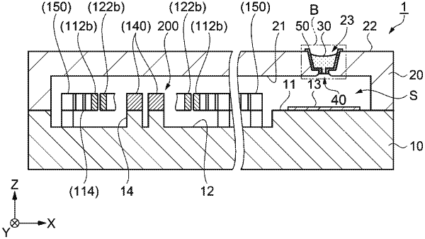
1. An electronic device comprising:
a substrate;
a functional element disposed on one surface of the substrate;
a lid body, the functional element being housed in a space covered by the lid body and the substrate, the lid body including:
a first surface facing the functional element;
a second surface at an opposite side of the first surface;
a first hole section including an inclined surface and a bottom surface on the second surface;
a second hole section piercing through the lid body between the first surface and the bottom surface of the first hole section and having an inner wall surface; and
a first joining section of the inclined surface and the bottom surface in the first hole section being a first curved surface along a vertical direction in a cross section of the inclined surface and the bottom surface of the first hole section, the lid body containing silicon; and
a sealing member that seals the first hole section communicating with the space,
wherein a curvature radius of the first curved surface is in a range of 5 nm and 50 μm.
|