| CPC G01N 1/24 (2013.01) [G01N 1/2273 (2013.01); G08B 3/10 (2013.01); G01N 1/2205 (2013.01)] | 20 Claims |
|
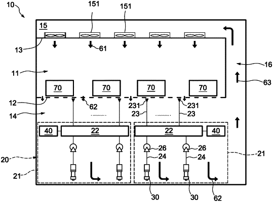
1. A method of monitoring a semiconductor fabrication facility, comprising:
collecting an ambient air in a clean room through a plurality of gas lines with their gas inlets arranged at a plurality of sampling positions in the clean room;
measuring a parameter of the ambient air by a plurality of metrology devices which are connected to the gas lines, wherein at least two of the sampling positions are measured simultaneously through at least two of the metrology devices; and
issuing a warning when the parameter detected by the metrology devices is outside a range of acceptable values.
|