US 11,891,720 B2
Gallium arsenide single crystal substrate and method for producing gallium arsenide single crystal substrate
Koji Uematsu, Osaka (JP); Issei Satoh, Osaka (JP); and Fumitake Nakanishi, Hyogo (JP)
Assigned to Sumitomo Electric Industries, Ltd., Osaka (JP)
Appl. No. 17/784,653
Filed by SUMITOMO ELECTRIC INDUSTRIES, LTD., Osaka (JP)
PCT Filed Sep. 1, 2020, PCT No. PCT/JP2020/033077
§ 371(c)(1), (2) Date Jun. 12, 2022,
PCT Pub. No. WO2021/176750, PCT Pub. Date Sep. 10, 2021.
Prior Publication US 2023/0002931 A1, Jan. 5, 2023
Int. Cl. B32B 3/00 (2006.01); C30B 29/42 (2006.01); C30B 33/02 (2006.01); G01N 23/2273 (2018.01)
CPC C30B 29/42 (2013.01) [C30B 33/02 (2013.01); G01N 23/2273 (2013.01)] 11 Claims
OG exemplary drawing
 
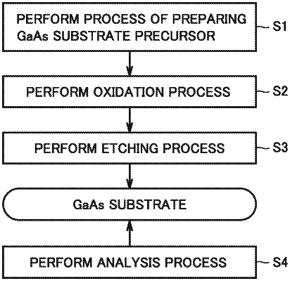
1. A gallium arsenide single crystal substrate having a main surface, wherein
a ratio of a number of As atoms existing as diarsenic trioxide to a number of As atoms existing as diarsenic pentoxide is greater than or equal to 2 when the main surface is measured by X-ray photoelectron spectroscopy, in which an X-ray having an energy of 150 eV is used and a take-off angle of a photoelectron is set to 5°, and
arithmetic average roughness Ra of the main surface is less than or equal to 0.3 nm.