| CPC C25D 17/001 (2013.01) [C25D 7/123 (2013.01); C25D 17/004 (2013.01); C25D 17/005 (2013.01); C25D 17/06 (2013.01)] | 10 Claims |
|
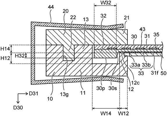
1. A semiconductor device manufacturing jig for electroplating a substrate,
the substrate including:
an inner part including a first surface and a second surface, the second surface being opposite to the first surface; and
an outer rim part surrounding the inner part, the outer rim part having a ring shape that protrudes further than the first surface in a direction perpendicular to the first surface,
the jig comprising a conductive member and a cover member, the substrate being clamped between the conductive member and the cover member,
the conductive member causing a current to flow in the inner part by contacting a portion of the first surface of the inner part without contacting the outer rim part, the conductive member including a contact part that contacts the portion of the first surface and,
the cover member having a ring shape, the cover member contacting the second surface of the inner part of the substrate at a side opposite to the first surface,
the conductive member having a groove that provides a space between the conductive member and the cover member, the outer rim part of the substrate being positioned in the space when the substrate is clamped between the conductive member and the cover member.
|