| CPC B81C 99/002 (2013.01) [H01L 21/67271 (2013.01); H01L 21/67294 (2013.01); H01L 24/95 (2013.01); H01L 2224/95133 (2013.01); H01L 2224/95145 (2013.01); H01L 2924/1461 (2013.01); Y10T 29/49133 (2015.01); Y10T 29/5313 (2015.01)] | 7 Claims |
|
1. An apparatus, comprising:
a memory configured to store control data;
a processing device, operatively coupled to the memory, the processing device configured to:
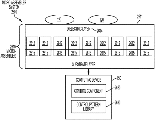
analyze a set of micro-objects located a surface of a micro-assembler, wherein the micro-assembler comprises an array of force generating pixels, wherein each force generating pixel in the array of force generating pixels comprises a phototransistor;
identify one or more geometric properties of the set of micro-objects;
divide the set of micro-objects into a first subset of micro-objects and a second-subset of micro-objects based on the one or more geometric properties and one or more control patterns, wherein the one or more control patterns indicate one or more force patterns on one or more portions of the array of force generating pixels;
form an optical image comprising a light pattern corresponding with the one or more control patterns; and
cause the optical image to be emitted over the array of force generating pixels to form the one or more force patterns.
|