| CPC B81B 7/007 (2013.01) [B81B 7/008 (2013.01); B81C 1/0023 (2013.01); B81C 2203/035 (2013.01); H01L 29/66 (2013.01)] | 20 Claims |
|
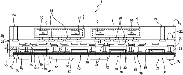
1. A device, comprising:
a coating region having a first surface and a second surface;
a dielectric region of a redistribution structure having a first surface, in contact with the first surface of the coating region, and a second surface opposite to the first surface of the dielectric region;
a die in the coating region;
a plurality of conductive regions in the coating region, extending to the first surface of the coating region, and electrically coupled to the die;
a plurality of conductive paths in the dielectric region of the redistribution structure and extending from the first surface of the dielectric region to the second surface of the dielectric region;
a plurality of conductive pillars extending outward from the second surface of the dielectric region of the redistribution structure and coupled to the plurality of conductive regions by the plurality of conductive paths;
a transduction structure including:
a plurality of pads in electrical contact with the plurality of conductive pillars; and
a plurality of membranes; and
a plurality of actuators electrically coupled to the plurality of pads.
|