| CPC B41J 29/377 (2013.01) [B41J 2/3358 (2013.01); B41J 2/1408 (2013.01); B41J 2202/08 (2013.01); H05K 7/20 (2013.01); H05K 7/20154 (2013.01); H05K 7/20163 (2013.01)] | 11 Claims |
|
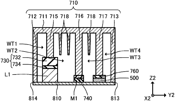
1. An electronic device comprising:
a substrate;
a first electronic component provided on the substrate;
a second electronic component provided on the substrate and having a thickness in a normal direction of the substrate smaller than that of the first electronic component;
a first heat conductive member in contact with the first electronic component;
a second heat conductive member in contact with the second electronic component; and
a heat sink attached to the substrate, wherein
the heat sink includes
a base portion provided so as to cover the first electronic component and the second electronic component and attached to the substrate,
a first protruding portion that protrudes from the base portion toward the first electronic component and is in contact with the first heat conductive member, and
a second protruding portion that protrudes from the base portion toward the second electronic component and is in contact with the second heat conductive member, and
a length of the first protruding portion in the normal direction is shorter than a length of the second protruding portion in the normal direction.
|