| CPC B23K 35/262 (2013.01) [B23K 1/0016 (2013.01); B23K 35/302 (2013.01); C23C 18/1637 (2013.01); C23C 18/32 (2013.01); B23K 2101/40 (2018.08); B23K 2103/12 (2018.08)] | 10 Claims |
|
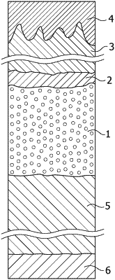
1. A solder joint comprising:
a solder joint layer having a melted solder material containing Sn as a main component and further containing Ag and/or Sb and/or Cu; and
a joined body including a Ni—P—Cu plating layer on a surface in contact with the solder joint layer, wherein
the Ni—P—Cu plating layer contains Ni as a main component and contains 0.5% by mass or greater and 8% by mass or less of Cu and 3% by mass or greater and 10% by mass or less of P,
the Ni—P—Cu plating layer has a microcrystalline layer at an interface with the solder joint layer, and the microcrystalline layer includes a phase containing microcrystals of a NiCuP ternary alloy, a phase containing microcrystals of (Ni,Cu)3P, and a phase containing microcrystals of Ni3P.
|