| CPC A24F 40/40 (2020.01) [H02M 3/1582 (2013.01)] | 12 Claims |
|
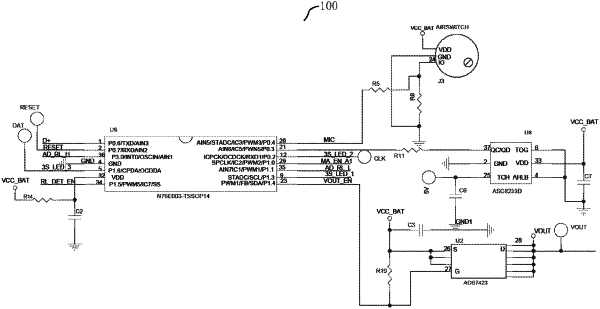
1. A voltage output circuit, wherein the voltage output circuit comprises:
a control chip (U6), the control chip (U6) comprises a first control signal input terminal (20), a second control signal input terminal (21), and a modulation signal output terminal (23), the first control signal input terminal (20) is connected to a first control signal output terminal (24) of a suction detection element (J3), the second control signal input terminal (21) is connected to a second control signal output terminal (37) of a touch sensing chip (U8), a touch input pin (25) of the touch sensing chip (U8) is connected to a touch panel;
a buck switch chip (U2), the buck switch chip (U2) comprises a first channel terminal (26), a first control terminal (27), and a second channel terminal (28), the first channel terminal (26) of the buck switch chip (U2) receives a system power supply voltage, the first control terminal (27) of the buck switch chip (U2) is connected to the modulation signal output terminal (23) of the control chip (U6);
when the first control signal input terminal (20) receives an effective level and/or the second control signal input terminal (21) receives an effective level, the modulation signal output terminal (23) of the control chip (U6) outputs a pulse width modulation signal to the first control terminal (27) of the buck switch chip (U2);
when the first control terminal (27) of the buck switch chip (U2) receives a pulse width modulation signal of an effective level, the first channel terminal (26) and the second channel terminal (28) are controlled to be conducted, and the second channel terminal (28) outputs a driving voltage with a voltage value thereof being less than a voltage value of the system power supply voltage.
|