US 11,871,685 B2
Resistive random-access memory (RRAM) device and forming method thereof
Wen-Jen Wang, Tainan (TW); Chun-Hung Cheng, Kaohsiung (TW); and Chuan-Fu Wang, Miaoli County (TW)
Assigned to UNITED MICROELECTRONICS CORP., Hsin-Chu (TW)
Filed by UNITED MICROELECTRONICS CORP., Hsin-Chu (TW)
Filed on Jul. 19, 2021, as Appl. No. 17/378,795.
Claims priority of application No. 202110641056.5 (CN), filed on Jun. 9, 2021.
Prior Publication US 2022/0399495 A1, Dec. 15, 2022
Int. Cl. H10N 70/00 (2023.01); H10N 70/20 (2023.01)
CPC H10N 70/841 (2023.02) [H10N 70/011 (2023.02); H10N 70/24 (2023.02); H10N 70/826 (2023.02); H10N 70/8833 (2023.02)] 20 Claims
OG exemplary drawing
 
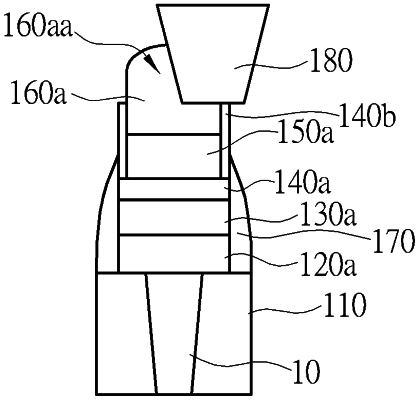
1. A resistive random-access memory (RRAM) device, comprising:
a bottom electrode, a resistive material layer, a high work function layer, a top electrode and a hard mask sequentially stacked on a substrate; and
high work function sidewall parts covering sidewalls of the top electrode and sidewalls of the hard mask, thereby constituting a RRAM cell.