| CPC H10N 70/253 (2023.02) [H10N 70/24 (2023.02); H10N 70/826 (2023.02); H10N 70/8413 (2023.02)] | 20 Claims |
|
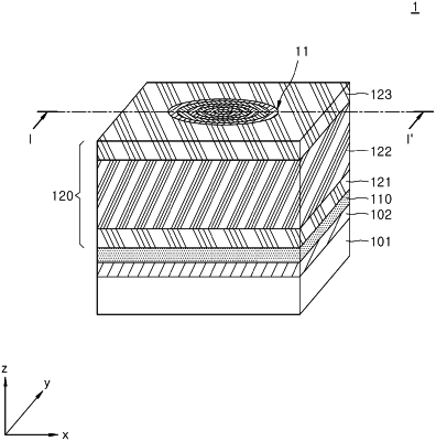
1. A semiconductor device comprising;
a substrate;
a gate structure disposed over the substrate, the gate structure including at least one gate electrode layer and at least one interlayer insulating layer that are alternately stacked over the substrate;
a hole pattern penetrating the gate structure over the substrate; and
a gate insulating layer, a channel layer, a resistor layer, and a resistance changing layer that are sequentially disposed on a sidewall surface of the gate structure within the hole pattern,
wherein each of the resistor layer and the resistance changing layer is disposed opposite to the gate insulating layer, based on the channel layer.
|