| CPC H10N 50/01 (2023.02) [H10B 61/00 (2023.02); H10N 50/80 (2023.02)] | 5 Claims |
|
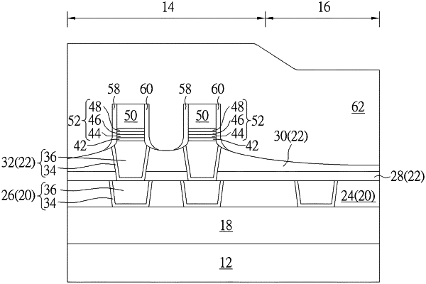
1. A method for fabricating a semiconductor device, comprising:
providing a substrate, wherein the substrate comprises a magnetoresistive random access memory (MRAM) region and a logic region;
forming a magnetic tunneling junction (MTJ) on the MRAM region;
forming a top electrode on the MTJ;
performing a flowable chemical vapor deposition (FCVD) process to form a first inter-metal dielectric (IMD) layer around the top electrode and the MTJ, wherein a top surface of the first IMD layer on the logic region is lower than a top surface of the first IMD layer on the MRAM region and higher than a top surface of the top electrode, and the top surface of the first IMD layer directly on top of the MTJ and the top surface of the first IMD layer adjacent to the MTJ on the MRAM region comprise a completely planar surface; and
performing a planarizing process to planarizing the first IMD layer after performing the FCVD process, wherein a height difference between the first IMD layer on the logic region and the first IMD layer on the MRAM region before the planarizing process is less than 400 Angstroms.
|