| CPC H10K 71/00 (2023.02) [H10K 50/822 (2023.02); H10K 50/844 (2023.02); H10K 59/122 (2023.02); H10K 59/124 (2023.02); H10K 59/35 (2023.02)] | 13 Claims |
|
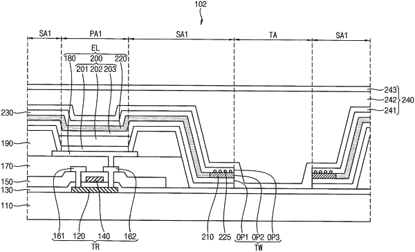
1. A display device, comprising:
a first electrode;
a second electrode overlapping the first electrode;
an emission layer disposed between the first electrode and the second electrode, overlapping the first electrode, and including a light emitting material;
an intervening layer directly contacting the second electrode, spaced from each of the first electrode and the emission layer, and including a fluorine compound;
a first encapsulation layer, wherein a first section of the first encapsulation layer overlaps the emission layer, and wherein the intervening layer is positioned between the second electrode and a second section of the first encapsulation layer; and
agglomerated particles disposed between the intervening layer and the first encapsulation layer and including a same material as the second electrode.
|