| CPC H10K 59/60 (2023.02) [H10K 50/858 (2023.02); H10K 59/124 (2023.02); H10K 59/65 (2023.02)] | 16 Claims |
|
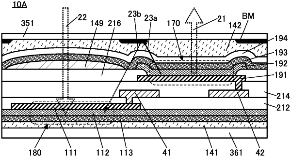
1. A display device comprising a display portion,
wherein the display portion comprises a first substrate, a second substrate, a light-receiving element, a transistor, and a light-emitting element,
wherein the light-receiving element, the transistor, and the light-emitting element are each positioned between the first substrate and the second substrate,
wherein the light-receiving element is positioned closer to the first substrate than the transistor is,
wherein the light-emitting element is positioned closer to the second substrate than the transistor is,
wherein the light-receiving element comprises a first electrode, a first layer comprising an organic compound over the first electrode, and a second electrode over the first layer,
wherein the light-emitting element comprises a third electrode, a second layer over the third electrode, and a fourth electrode over the second layer,
wherein the second electrode is configured to transmit light,
wherein the fourth electrode is configured to transmit light, and
wherein the transistor is electrically connected to the light-emitting element.
|