| CPC H10K 59/353 (2023.02) [H10K 59/00 (2023.02); H10K 59/121 (2023.02); H10K 59/131 (2023.02)] | 14 Claims |
|
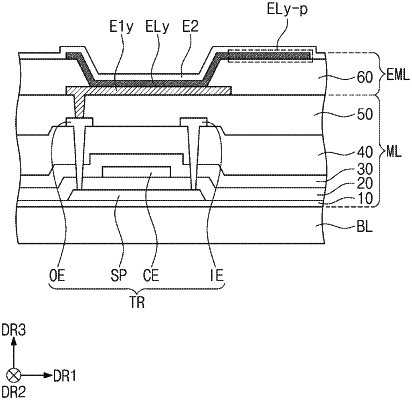
1. A display panel, comprising:
a base layer that includes a first region and a second region, the second region including a first sub-region and a second sub-region, wherein the second sub-region corresponds to a transmission region;
a plurality of first pixels on the first region; and
a plurality of second pixels on the first sub-region, wherein
each of the plurality of first pixels includes a first pixel electrode, a first emission layer on the first pixel electrode, and a first common electrode on the first emission layer,
each of the plurality of second pixels includes a second pixel electrode, a second emission layer on the second pixel electrode, and a second common electrode on the second emission layer, and
the second pixel electrode is shifted relative to the second emission layer in a direction away from the second sub-region such that the second pixel electrode does not overlap an edge of the second emission layer closest among all edges of the second emission layer to the second sub-region.
|