| CPC H10K 59/1315 (2023.02) [H10K 59/1201 (2023.02)] | 12 Claims |
|
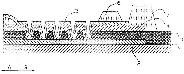
1. An array substrate, comprising:
a base substrate comprising a display area and a border area around the display area; and
a signal line and an electrode line located in the border area of the base substrate, wherein
the signal line is arranged in a same layer as a source-drain electrode layer in the display area, and the electrode line is arranged in a same layer as an anode layer in the display area; and
the electrode line is overlapped on a surface of the signal line away from the base substrate, overlapping surfaces of the signal line and the electrode line are two concave-convex surfaces fitted to each other,
wherein the signal line comprises a first body parallel to the base substrate and a plurality of first recesses recessed from a surface of the first body away from the base substrate in a direction towards the base substrate;
the electrode line comprises a second body parallel to the base substrate and a plurality of first bumps protruding from a surface of the second body facing the signal line in a direction towards the signal line;
the plurality of first recesses and the plurality of first bumps are arranged in one-to-one correspondence, and a surface of each of the first recesses and a surface of the bump corresponding to said each of the first recess are completely fitted to each other to form the concave-convex surfaces, and
wherein the plurality of first recesses protrude from a surface of the first body facing the base substrate in a direction towards the base substrate;
the array substrate further comprises: an interlayer dielectric layer located on the base substrate, wherein the signal line and the electrode line are successively laminated on the interlayer dielectric layer, and a part of the interlayer dielectric layer in the border area has a plurality of grooves, and portions of the plurality of first recesses protruding from the first body and facing the surface of the base substrate are arranged in the plurality of grooves in one-to-one correspondence,
wherein the array substrate further comprises: a conductive layer located in the border area on the base substrate, wherein the interlayer dielectric layer is located on the conductive layer, the plurality of grooves pass through the interlayer dielectric layer, and the plurality of first recesses electrically contact the conductive layer through the grooves respectively, a thickness of the first body of the signal line in a direction perpendicular to the base substrate is greater than a thickness of a part of the signal line located within the first recess; and a border, away from the display area, of an orthographic projection of the conductive layer on the base substrate coincides with a border, away from the display area, of an orthographic projection of the signal line on the base substrate.
|