| CPC H10K 59/131 (2023.02) [H10K 59/122 (2023.02); H10K 59/1213 (2023.02); H10K 59/1216 (2023.02); H10K 59/124 (2023.02)] | 20 Claims |
|
1. A display panel, comprising:
a base substrate comprising a display area and a peripheral area surrounding the display area;
a plurality of sub-pixels located at the display area, wherein each of the plurality of sub-pixels comprises an anode located on one side of the base substrate and a light-emitting function layer located on one side of the anode away from the base substrate;
a driving circuit located at the peripheral area, and configured to output a gate driving signal and a light-emitting control scanning signal to the plurality of sub-pixels;
a power line located on one side of the driving circuit away from the display area;
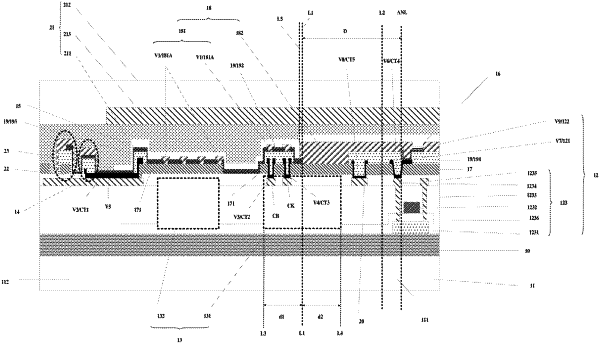
a connection layer electrically connected to the power line and located on one side of the driving circuit and the power line away from the base substrate, wherein an orthographic projection of the connection layer on the base substrate partially overlaps with an orthographic projection of the driving circuit on the base substrate, and a minimum distance between an edge of the orthographic projection of the connection layer on the base substrate close to the display area and an edge of an orthographic projection of the anode, which is closest to an edge of the display area of a plurality of anodes of the plurality of sub-pixels, on the base substrate ranges from 150 microns to 250 microns; and
a cathode electrically connected to the connection layer, located at the display area and the peripheral area, and located on one side of the light-emitting function layer and the connection layer away from the base substrate,
wherein the driving circuit comprises a gate driving circuit located between the display area and the power line, and configured to output the gate drive signal to the plurality of sub-pixels, wherein the edge of the orthographic projection of the connection layer on the base substrate close to the display area is at leas partially located within an orthographic projection of the gate driving circuit on the base substrate, and
wherein the gate driving circuit comprises a plurality of a gate driving units, each of the plurality of gate driving units comprising:
a first gate driving sub-circuit comprising an input terminal of the each of the plurality of gate driving units, and
a second gate driving sub-circuit electrically connected to the first gate driving sub-circuit, located between the first gate driving sub-circuit and the display area, and comprising an output terminal of the each of the plurality of gate driving units, wherein an orthographic projection of the second gate driving sub-circuit on the base substrate overlaps with the edge of the orthographic projection of the connection layer on the base substrate close to the display area.
|