| CPC H10K 59/131 (2023.02) [H10K 59/1201 (2023.02)] | 18 Claims |

|
1. A display substrate, comprising:
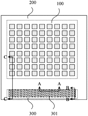
a display area, a peripheral area and a binding area, the peripheral area being located at a periphery of the display area, the binding area being located on one side of the peripheral area away from the display area; the display substrate comprising a silicon-based substrate and an array structure layer arranged on the silicon-based substrate; a driving transistor and a first power line being arranged in the silicon-based substrate in the display area, a light emitting element being disposed on the array structure layer in the display area, a first electrode of the driving transistor being connected with the first power line, and a second electrode of the driving transistor being connected with an anode of the light emitting element; a power supply electrode and a second power line being arranged in the silicon-based substrate in the peripheral area, the power supply electrode being connected with the second power line; and a bonding pad assembly being disposed in the silicon-based substrate in the binding area, a binding platform being arranged on the array structure layer in the binding area, the binding platform being connected with the bonding pad assembly by a conductive pillar, the bonding pad assembly being connected with the first power line and the second power line, the binding platform and the anode of the light emitting element being arranged on the same layer, and the binding platform being configured to be bound to a flexible printed circuit.
|