| CPC H10K 59/131 (2023.02) [H10K 59/124 (2023.02); H10K 59/126 (2023.02); G09G 3/32 (2013.01); G09G 2300/0809 (2013.01)] | 12 Claims |
|
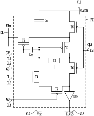
1. A display device comprising:
a first semiconductor layer disposed on a substrate;
a first insulating layer disposed on the first semiconductor layer;
a scan line disposed on the first insulating layer, the scan line carrying a scan signal;
a second insulating layer disposed on the scan line;
an inverted scan line disposed on the second insulating layer, the inverted scan line carrying an inverted version of the scan signal;
a third insulating layer disposed on the inverted scan line;
a second semiconductor layer disposed on the third insulating layer;
a fourth insulating layer disposed on the second semiconductor layer;
an initializing voltage line disposed on the fourth insulating layer and overlapping the scan line;
a first transistor including a channel disposed in the first semiconductor layer, the first transistor receiving a gate signal through the scan line;
a second transistor including a channel disposed in the second semiconductor layer, the second transistor receiving a gate signal through the inverted scan line;
a data line extending in a second direction intersecting a first direction, and
a shielding electrode electrically connected to the initializing voltage line and extending parallel to the data line;
a fifth insulating layer disposed on the initializing voltage line;
a third transistor including a channel disposed in the first semiconductor layer; and
a first connecting member electrically connecting a gate electrode of the third transistor and a drain electrode of the second transistor and disposed on the fifth insulating layer, wherein
the initializing voltage line extends in the first direction parallel to the scan line,
the data line and the shielding electrode are disposed on the fifth insulating layer,
the shielding electrode is electrically connected to the initializing voltage line through an opening of the fifth insulating layer, and
the first connecting member does not overlap the inverted scan line.
|