US 11,871,608 B2
Display device
Byunghan Yoo, Yongin-si (KR); Geebum Kim, Yongin-si (KR); Sangwoo Kim, Yongin-si (KR); Chaungi Choi, Yongin-si (KR); Jungha Son, Yongin-si (KR); Taekyung Ahn, Yongin-si (KR); Kijune Lee, Yongin-si (KR); and Jaeik Lim, Yongin-si (KR)
Assigned to Samsung Display Co., Ltd., Yongin-si (KR)
Appl. No. 17/417,422
Filed by Samsung Display Co., Ltd., Yongin-si (KR)
PCT Filed Oct. 14, 2019, PCT No. PCT/KR2019/013432
§ 371(c)(1), (2) Date Jun. 23, 2021,
PCT Pub. No. WO2020/138665, PCT Pub. Date Jul. 2, 2020.
Claims priority of application No. 10-2018-0171135 (KR), filed on Dec. 27, 2018.
Prior Publication US 2022/0085331 A1, Mar. 17, 2022
Int. Cl. H10K 50/85 (2023.01); H10K 59/00 (2023.01)
CPC H10K 50/85 (2023.02) [H10K 59/00 (2023.02)] 27 Claims
OG exemplary drawing
 
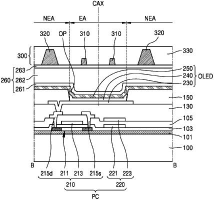
1. A display device comprising:
a pixel electrode on a substrate;
an insulating layer defining an emission area via an opening that covers edges of the pixel electrode and exposes a center portion of the pixel electrode;
a first light extraction pattern on the pixel electrode, the first light extraction pattern having a side surface inclined at a first angle; and
a second light extraction pattern surrounding the first light extraction pattern on an outer portion of the first light extraction pattern, the second light extraction pattern having a side surface inclined at a second angle that is less than the first angle.