| CPC H10K 50/844 (2023.02) [H10K 59/122 (2023.02); H10K 71/00 (2023.02); H10K 59/1201 (2023.02); H10K 2102/351 (2023.02)] | 20 Claims |
|
1. A display panel, comprising:
a display area, an opening area, and an isolation area between the display area and the opening area, the isolation area being at least partially arranged around the opening area;
a base substrate;
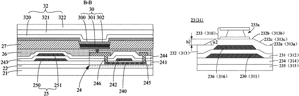
a driving circuit layer comprising a thin film transistor and a storage capacitor that are formed on the base substrate and located in the display area, in which the thin film transistor comprises a gate electrode, a first gate insulating layer formed at a side of the gate electrode away from the base substrate, an interlayer dielectric layer formed at a side of the first gate insulating layer away from the base substrate, and source and drain electrodes formed at a side of the interlayer dielectric layer away from the base substrate, wherein the storage capacitor comprises a first electrode plate arranged on the same layer as the gate electrode and a second electrode plate positioned between the first gate insulating layer and the interlayer dielectric layer;
a first isolation column formed on the base substrate and located in the isolation area; in which the first isolation column is arranged around the opening area and comprises a first metal layer, a first insulating layer formed at a side of the first metal layer away from the base substrate, a second insulating layer formed at a side of the first insulating layer away from the base substrate, and a second metal layer formed at a side of the second insulating layer away from the base substrate;
wherein the first metal layer is arranged on the same layer as the first electrode plate or the second electrode plate; the first insulating layer is arranged in the same layer as the first gate insulating layer; the second insulating layer is arranged on the same layer as the interlayer dielectric layer, and comprises a first portion, a second portion and a first inclined portion connecting the first portion and the second portion, a slope angle of the first inclined portion is less than 90°; the second metal layer is arranged on the same layer as the source and drain electrodes and is located at a side of the second portion away from the base substrate, and a notch surrounding the opening area is arranged at a side facing towards the display area and/or a side facing towards the opening area.
|