| CPC H10K 50/82 (2023.02) [H10K 50/844 (2023.02); H10K 59/122 (2023.02); H10K 59/124 (2023.02); H10K 71/00 (2023.02)] | 20 Claims |
|
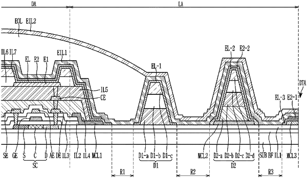
1. A display device comprising:
a substrate including an opening area, a peripheral area surrounding the opening area, and a display area surrounding the peripheral area;
a transistor overlapping the display area and disposed on the substrate;
a first electrode electrically connected to the transistor;
an intermediate layer and a second electrode disposed on the first electrode and extending to the peripheral area; and
a first metal layer overlapping the intermediate layer and the second electrode in the peripheral area,
wherein an end of the first metal layer and an end of the second electrode extended from the display area and connected to the second electrode overlapping the display area are aligned, and
an end of the intermediate layer is protruded more than the end of the first metal layer such that a bottom surface of the end of the intermediate layer that protrudes more than the end of the first metal layer is disposed at a same distance above the substrate as a bottom surface of the first metal layer.
|