| CPC H10K 50/813 (2023.02) [H01L 33/50 (2013.01); H10K 50/822 (2023.02); H10K 59/122 (2023.02); H10K 59/124 (2023.02); H10K 71/00 (2023.02)] | 12 Claims |
|
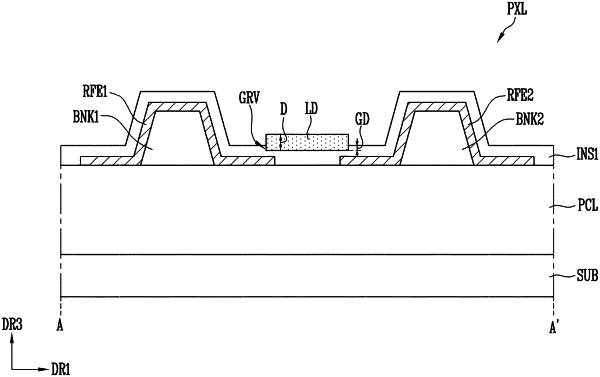
1. A display device comprising:
a substrate;
a first electrode and a second electrode on the substrate, the first electrode and the second electrode being arranged on a same layer to be spaced apart from each other;
a first insulating layer on the first electrode and the second electrode; and
a light emitting element on the first insulating layer, the entirety of the light emitting element overlaps with the first insulating layer,
wherein the first insulating layer defines a groove concave toward the substrate,
wherein the light emitting element is in the groove, and
wherein an upper portion of the groove is lower than an upper surface of the light emitting element, and is higher than a lower surface of the light emitting element.
|