| CPC H10B 53/30 (2023.02) [H01L 21/76802 (2013.01); H01L 23/528 (2013.01); H01L 23/535 (2013.01); H01L 23/53209 (2013.01); H01L 23/53228 (2013.01); H01L 23/53242 (2013.01); H01L 23/53257 (2013.01); H01L 28/55 (2013.01); H01L 28/60 (2013.01); H01L 28/65 (2013.01); H03K 19/185 (2013.01); H10B 53/10 (2023.02)] | 16 Claims |
|
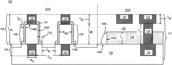
1. A device comprising:
a first region comprising:
a first conductive interconnect within a first level; and
a second level above the first level, the second level comprising:
a ferroelectric memory device comprising a first height and further comprising a cylindrical shape, the ferroelectric memory device above the first conductive interconnect;
an encapsulation layer on a sidewall of the ferroelectric memory device; and
a via electrode on the ferroelectric memory device, wherein the via electrode comprises a second height;
a second region adjacent to the first region, the second region comprising an interconnect structure, the interconnect structure comprising:
a second conductive interconnect within the first level;
an etch stop layer comprising a dielectric material in the second level;
a metal line above the etch stop layer, wherein the metal line is within the second level and wherein the metal line comprises a third height; and
a via structure coupling the metal line with the second conductive interconnect, wherein the via structure is in the second level and comprises a fourth height, wherein a combined sum of the first height and the second height is equal to a combined sum of the third height and the fourth height; and
a portion of one or more layers of the ferroelectric memory device adjacent to a sidewall of the etch stop layer at a boundary between the first region and the second region.
|