US 11,871,582 B2
Vertical transistor, integrated circuitry, method of forming a vertical transistor, and method of forming integrated circuitry
Hung-Wei Liu, Meridian, ID (US); Vassil N. Antonov, Boise, ID (US); Ashonita A. Chavan, Boise, ID (US); Darwin Franseda Fan, Boise, ID (US); Jeffery B. Hull, Boise, ID (US); Anish A. Khandekar, Boise, ID (US); Masihhur R. Laskar, Boise, ID (US); Albert Liao, Boise, ID (US); Xue-Feng Lin, Boise, ID (US); Manuj Nahar, Boise, ID (US); and Irina V. Vasilyeva, Boise, ID (US)
Assigned to Micron Technology, Inc., Boise, ID (US)
Filed by Micron Technology, Inc., Boise, ID (US)
Filed on Jan. 31, 2022, as Appl. No. 17/589,310.
Application 17/589,310 is a division of application No. 17/027,046, filed on Sep. 21, 2020, granted, now 11,264,395.
Prior Publication US 2022/0157837 A1, May 19, 2022
Int. Cl. H10B 53/20 (2023.01); H01L 29/78 (2006.01); H01L 29/66 (2006.01); H01L 29/10 (2006.01); H01L 21/223 (2006.01); H10B 51/20 (2023.01); H10B 51/30 (2023.01); H10B 53/30 (2023.01)
CPC H10B 53/20 (2023.02) [H01L 21/223 (2013.01); H01L 29/1037 (2013.01); H01L 29/66666 (2013.01); H01L 29/7827 (2013.01); H10B 51/20 (2023.02); H10B 51/30 (2023.02); H10B 53/30 (2023.02)] 14 Claims
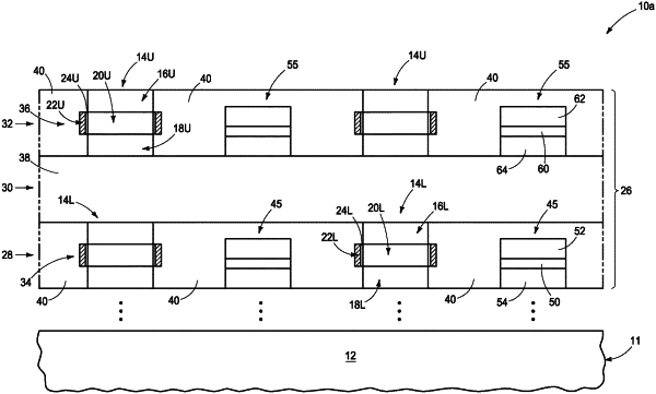
OG exemplary drawing
 
1. A method of forming a vertical transistor comprising a top source/drain region, a bottom source/drain region, a channel region vertically between the top and bottom source/drain regions, and a gate operatively laterally-adjacent the channel region, the method comprising:
in multiple time-spaced microwave annealing steps, microwave annealing at least the channel region; the multiple time-spaced microwave annealing steps reducing average concentration of elemental-form H in the channel region from what it was before start of the multiple time-spaced microwave annealing steps, the reduced average concentration of elemental-form H being 0.005 to less than 1 atomic percent.