| CPC H10B 53/20 (2023.02) [H01L 23/5226 (2013.01); H01L 23/5283 (2013.01); H01L 29/42392 (2013.01); H10B 51/10 (2023.02); H10B 51/20 (2023.02); H10B 53/00 (2023.02); H10B 53/10 (2023.02)] | 20 Claims |
|
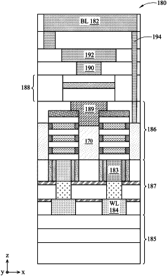
1. A memory cell of a memory array, comprising:
a substrate;
an interconnect structure bonded to the substrate via a bond interface layer, the interconnect structure coupled to a word line of the memory array;
a field effect transistor (FET) on top of the interconnect structure and electrically coupled to the interconnect structure via a gate contact;
a ferroelectric capacitor on the FET;
a source/drain contact electrically coupling the ferroelectric capacitor to a source/drain region of the FET; and
a ground contact to the ferroelectric capacitor.
|