| CPC H10B 51/30 (2023.02) [H01L 21/764 (2013.01); H01L 29/0649 (2013.01); H10B 41/27 (2023.02); H10B 41/35 (2023.02); H10B 43/27 (2023.02); H10B 43/35 (2023.02); H10B 51/20 (2023.02)] | 7 Claims |
|
1. A three-dimensional memory device, comprising:
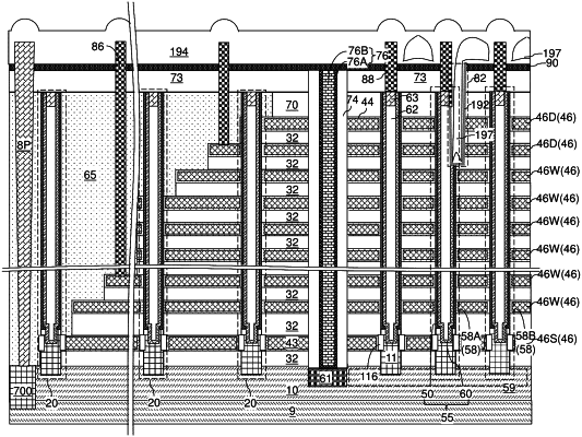
an alternating stack of insulating layers and electrically conductive layers located over a substrate, wherein the electrically conductive layers comprise word-line-level electrically conductive layers and drain-select-level electrically conductive layers overlying the word-line-level electrically conductive layers;
an array of memory opening fill structures located within an array of memory openings vertically extending through the alternating stack;
a drain-select-level isolation structure vertically extending through the drain-select-level electrically conductive layers and having an effective dielectric constant that is less than 3.9;
a contact-level dielectric layer overlying the alternating stack and the array of memory opening fill structures;
drain contact via structures vertically extending through the contact-level dielectric layer and contacting a top surface of a respective one of the memory opening fill structures;
a first backside trench fill structure laterally extending along the first horizontal direction and contacting first sidewalls of each layer within the alternating stack; and
a second backside trench fill structure laterally extending along the first horizontal direction and laterally spaced from the first backside trench fill structure and contacting second sidewalls of each layer within the alternating stack,
wherein:
the array of memory opening fill structures comprises two rows of first memory opening fill structures that are arranged along a first horizontal direction;
each of the first memory opening fill structures comprises a respective planar straight sidewall in contact with a respective portion of a pair of straight sidewalls of the drain-select-level isolation structure; and
top surfaces of the first backside trench fill structure and the second backside trench fill structure are located within a horizontal plane including a top surface of the contact-level dielectric layer; and
further comprising a capping dielectric material layer comprising a horizontally-extending portion that overlies the top surface of the contact-level dielectric layer, wherein the drain-select-level isolation structure comprises a vertically-extending portion of the capping dielectric material layer.
|