| CPC H10B 43/27 (2023.02) [H01L 21/0214 (2013.01); H01L 21/0217 (2013.01); H01L 21/02164 (2013.01); H01L 21/02236 (2013.01); H01L 29/40114 (2019.08); H01L 29/40117 (2019.08); H01L 29/4991 (2013.01); H01L 29/513 (2013.01); H01L 29/517 (2013.01); H01L 29/7883 (2013.01); H01L 29/792 (2013.01); H10B 41/27 (2023.02)] | 23 Claims |
|
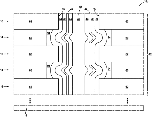
1. A method of forming an integrated structure, comprising:
forming a vertical stack of alternating first and second levels; the first levels comprising first material and the second levels comprising second material;
forming an opening to extend through the stack, the opening having a peripheral sidewall;
forming charge-blocking material adjacent the peripheral sidewall;
forming charge-storage material adjacent the charge-blocking material;
forming gate-dielectric material adjacent the charge-storage material;
forming channel material adjacent the gate-dielectric material;
removing the second material to leave first voids;
forming conductive levels within the first voids; the conductive levels having front ends with front surfaces; the front surfaces facing the charge blocking material;
after the forming of the charge-blocking material, forming high-k dielectric material to be between said front surfaces and the charge-blocking material; the high-k dielectric material being configured as first segments which are vertically-spaced from one another, with said first segments being along the front surfaces of the conductive levels and not wrapping around the front ends of the conductive levels;
removing the first material to leave second voids; and
extending the second voids through the charge-storage material to divide the charge-storage material into vertically-spaced segments.
|