US 11,871,571 B2
Nonvolatile memory device and method for fabricating the same
Soodoo Chae, Seongnam-si (KR); Myoungbum Lee, Seoul (KR); HuiChang Moon, Yongin-si (KR); Hansoo Kim, Suwon-si (KR); JinGyun Kim, Yongin-si (KR); Kihyun Kim, Hwaseong-si (KR); Siyoung Choi, Seongnam-si (KR); and Hoosung Cho, Yongin-si (KR)
Assigned to Samsung Electronics Co., Ltd., Suwon-si (KR)
Filed by Samsung Electronics Co., Ltd., Suwon-si (KR)
Filed on Nov. 2, 2021, as Appl. No. 17/517,137.
Application 17/517,137 is a continuation of application No. 17/497,417, filed on Oct. 8, 2021.
Application 17/497,417 is a continuation of application No. 16/708,482, filed on Dec. 10, 2019, granted, now 11,387,249.
Application 16/708,482 is a continuation of application No. 15/634,597, filed on Jun. 27, 2017, granted, now 10,546,872, issued on Jan. 28, 2020.
Application 15/634,597 is a continuation of application No. 14/973,182, filed on Dec. 17, 2015, granted, now 9,735,170, issued on Aug. 15, 2017.
Application 14/973,182 is a continuation of application No. 14/027,599, filed on Sep. 16, 2013, granted, now 9,245,839, issued on Jan. 26, 2016.
Application 14/027,599 is a continuation of application No. 12/592,869, filed on Dec. 3, 2009, granted, now 8,541,831, issued on Sep. 24, 2013.
Claims priority of application No. 10-2008-0121886 (KR), filed on Dec. 3, 2008; and application No. 10-2009-0016406 (KR), filed on Feb. 26, 2009.
Prior Publication US 2022/0059567 A1, Feb. 24, 2022
Int. Cl. H10B 43/27 (2023.01); H10B 43/10 (2023.01); H10B 43/20 (2023.01); H10B 43/50 (2023.01); H01L 23/498 (2006.01); H01L 23/535 (2006.01); H01L 29/40 (2006.01); H01L 29/423 (2006.01); H01L 23/522 (2006.01)
CPC H10B 43/27 (2023.02) [H01L 23/49844 (2013.01); H01L 23/5226 (2013.01); H01L 23/535 (2013.01); H01L 29/408 (2013.01); H01L 29/4234 (2013.01); H10B 43/10 (2023.02); H10B 43/20 (2023.02); H10B 43/50 (2023.02); H01L 2924/0002 (2013.01)] 10 Claims
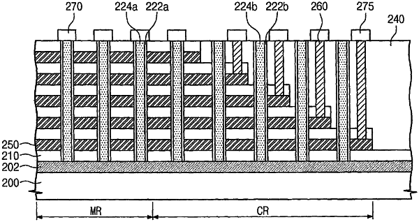
OG exemplary drawing
 
1. A method of fabricating a three-dimensional semiconductor device, comprising:
preparing a substrate including a first region and a second region;
forming a mold structure comprising first layers and second layers alternately stacked on the substrate,
patterning a portion of the mold structure to form a staircase structure on the second region;
forming a planarized dielectric layer covering the staircase structure of the mold structure;
forming a plurality of vertical patterns on the first region;
forming a plurality of supporters on the second region; and
removing the second layers to form gate regions between the first layers, the gate regions exposing portions of each of the vertical patterns and portions of each of the supporters; and
forming gate electrodes in the gate regions.