| CPC H10B 12/488 (2023.02) [H01L 21/76224 (2013.01); H01L 21/76877 (2013.01); H10B 12/30 (2023.02)] | 20 Claims |
|
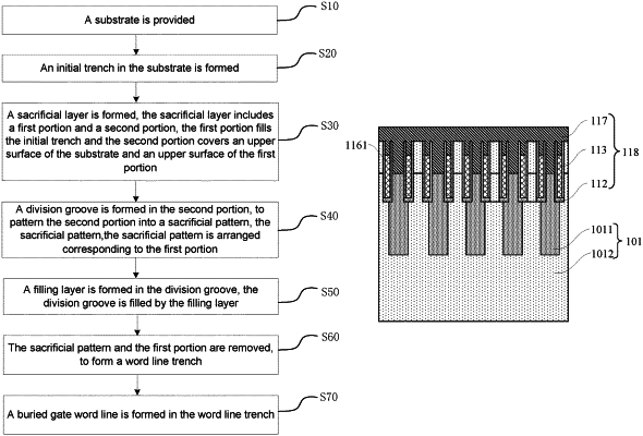
1. A method for manufacturing a semiconductor structure, comprising:
providing a substrate;
forming an initial trench in the substrate;
forming a sacrificial layer, the sacrificial layer comprising a first portion and a second portion, the first portion filling the initial trench and the second portion covering an upper surface of the substrate and an upper surface of the first portion;
forming a division groove in the second portion, to pattern the second portion into a sacrificial pattern, the sacrificial pattern being arranged corresponding to the first portion;
forming a filling layer in the division groove, the filling layer filling the division groove;
removing the sacrificial pattern and the first portion, to form a word line trench; and
forming a buried gate word line in the word line trench.
|